With our ISA-PLAN® technology, the elements of a precision and power resistor are etched from the films of our resistance alloys (MANGANIN®, ZERANIN®), which are electrically isolated and applied to a good heat-conducting metal substrate. The planar structures of our precision and power resistors and an optimized current density distribution allow for low-inductance designs and very low thermal internal resistance. An optimized current density distribution thus prevents the risk of hot spots.
Currently seven ISA-PLAN® SMD product series are available in addition to the conventional 2 and 4-wire current measuring resistors. The application options here are very diverse.
A SMD resistor of the ISA-PLAN® product series can and is used in the automotive, power electronics,drive electronics, energy measurement, medical technology and aviation and aerospace industries among others.
Production process of ISA-PLAN®-Resistors
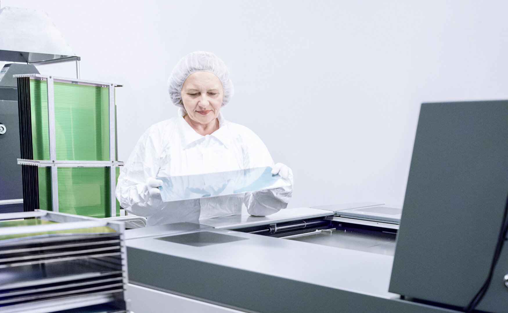
The production process of a resistor produced in the ISA-PLAN® technology begins with the bonding of the MANGANIN® or ZERANIN® film to a metal substrate made of copper or anodized aluminum. The high-temperature resistant bond is optimized with respect to the bond, isolation and above all low heat resistance between the resistor film and substrate. The resistor film and the substrate are vacuum-laminated at high pressure and high temperature after a pre-treatment. This guarantees a constant bonding without air inclusions.
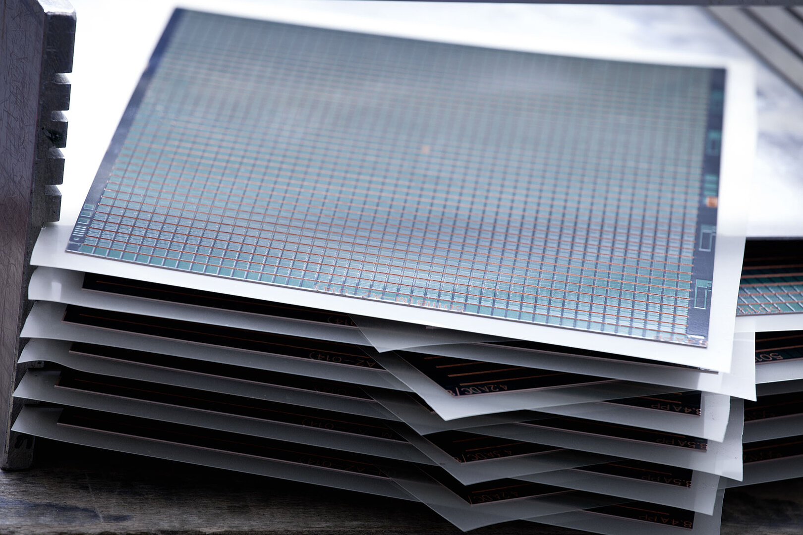
After cleaning, marking and the fitting hole punching, the panels undergo a photolithography process where individual structures of the low-resistance resistors are already defined. The entire assembly in conjunction with the etching technology allows for the production of an ideal four-wire SMD resistor in the low-resistance range.
The influence of the copper-connection resistor on the resistance value and the temperature coefficient of the components is eliminated with a four-wire resistor, thus guaranteeing the highest level of reproducibility. Influences of the solder point quality on the resistance value are thus excluded. With a two-wire resistor, a virtual four-wire connection can be realized together with the layout of the printed circuit board. This connection is very similar to the ideal four-wire resistor.
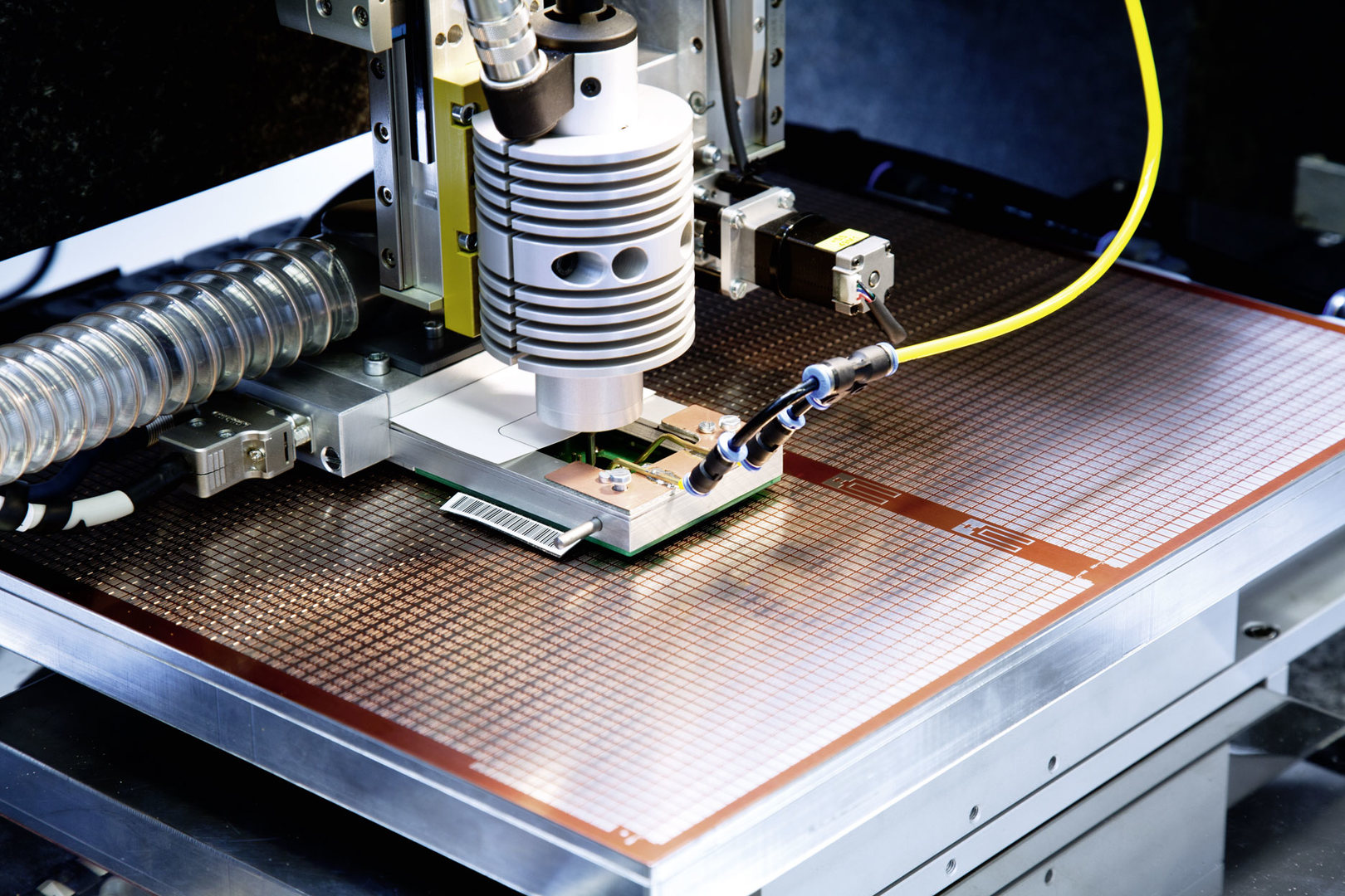
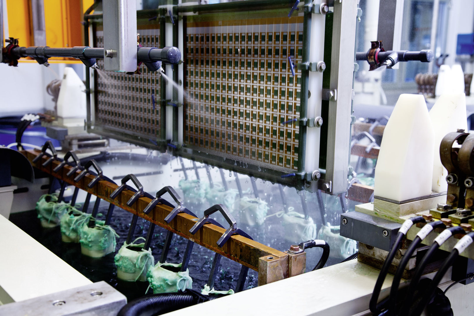
After the etching process, additional chemical treatments follow as well as largely automated processes, such as laser processing and adjustment. Power and precision resistors are tested under electric pulse load with a subsequent evaluation of the IR image in order to detect weak points in the etching structure. The low-resistance SMD resistors are separated from the substrate (panel) through lasering, punching or sawing.
The final process steps are fully automated, such as cleaning, resistance measurement, labeling and packaging. Every precision and power resistor is packaged in the webbing for the automatic SMD assembly. The finished inductors are welded into film to maintain the solderability and are back-gassed with nitrogen. Each inductor is marked with a bar code in order to allow the traceability of all product and production-related data. If desired, additional labeling is of course possible with a customer-specific part number.