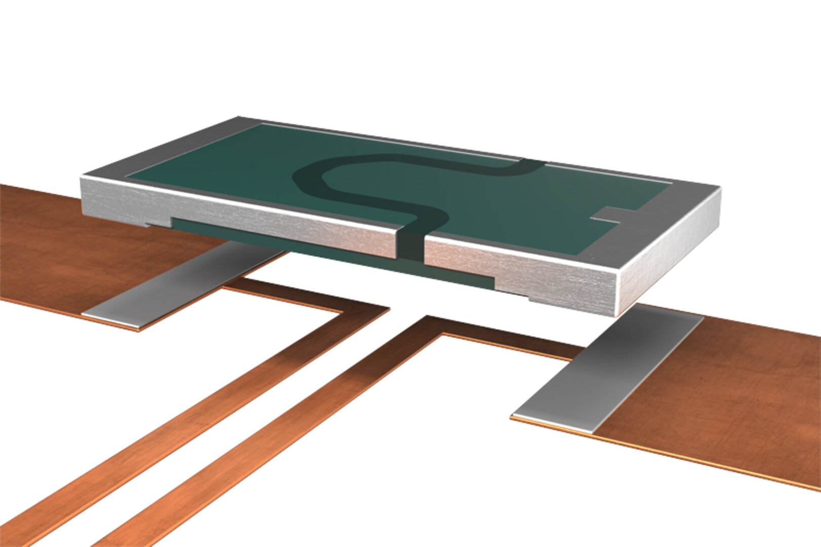
SMD steht für surface-mounted-device (oberflächenmontiertes Bauelement). Mittels ihrer Anschlussflächen werden die SMD-Bauteile direkt auf eine Leiterplatte gelötet. Unsere SMD montierbaren Präzisions- und Leistungswiderstände bieten Ihnen zahlreiche Vorteile in Standardbauformen.
Für Datenblätter mit Bildern und detaillierten Informationen über unsere Produkte im Bereich der Präzisions- und Leistungswiderstände, klicken Sie bitte hier.
| Typ | Bild | Beschreibung | Bauform | Leistung | Toleranz | TK | Widerstand (min) | Widerstand (max) | Download |
| BRS | 2-Leiter-Widerstand aus Verbundmaterial. Ideal für den Einsatz auf DCB oder Keramik. Platzsparende Bauart. | 3812 | 2 W | 1 % | 100 ppm/K | 0.002 Ω | 0.025 Ω | Download | |
| BVB | 4-Leiter-Widerstand aus Verbundmaterial. Ideal für den Einsatz auf DCB oder Keramik. Platzsparende Bauart. | 2725 | 12 W | 1 % | 20 ppm/K | 0.0002 Ω | 0.005 Ω | Download | |
| BVE | 2-Leiter-Widerstand mit großen Anschlüssen für hohe Leistung. | 5930 | 15 W | 1 % | 50 ppm/K | 0.0001 Ω | 0.003 Ω | Download | |
| BVH | Massive Kupferanschlüsse | 3820 | 5 W | 3 % | 300 ppm/K | 0.0003 Ω | 0.0005 Ω | Download | |
| BVN | 4-Leiter-Widerstand aus Verbundmaterial. Ideal für den Einsatz auf DCB oder Keramik. Platzsparende Bauart. | 1216 | 10 W | 1 % | 50 ppm/K | 0.0003 Ω | 0.003 Ω | Download | |
| BVR | 4-Leiter-Widerstand aus Verbundmaterial. Ideal für den Einsatz auf DCB. | 4026 | 12 W | 1 % | 20 ppm/K | 0.0002 Ω | 0.003 Ω | Download | |
| BVS | 2-Leiter-Widerstand aus Verbundmaterial. | 3920 | 12 W | 1 % | 50 ppm/K | 0.0002 Ω | 0.005 Ω | Download | |
| BVT | 2-Leiter-Widerstand aus Verbundmaterial. | 2512 | 10 W | 1 % | 50 ppm/K | 0.0003 Ω | 0.0068 Ω | Download | |
| BVZ | 2-Leiter-Widerstand aus Verbundmaterial. Ideal für den Einsatz auf DCB oder Keramik. Platzsparende Bauart. | 4026 | 13 W | 1 % | 60 ppm/K | 0.000525 Ω | 0.003 Ω | Download | |
| CLK | NEU: 2-Leiter-Widerstand. Querkontaktiert. Große Lötpads. Niedrige Widerstandswerte. | 0612 | 3 W | 1 % | 50 ppm/K | 0.001 Ω | 0.010 Ω | Download | |
| CLP | NEU: 2-Leiter-Widerstand. Querkontaktiert. Große Lötpads. Niedrige Widerstandswerte. | 1020 | 5 W | 1 % | 50 ppm/K | 0.002 Ω | 0.010 Ω | Download | |
| CMK | 2-Leiter-Widerstand für mittlere Leistungsanforderungen. Niedriger TK. | 1206 | 4 W | 1 % | 50 ppm/K | 0.005 Ω | 0.100 Ω | Download | |
| CMP | 2-Leiter-Widerstand für mittlere Leistungsanforderungen. Niedriger TK. | 2010 | 2 W | 1 % | 50 ppm/K | 0.010 Ω | 0.500 Ω | Download | |
| CMS | 2-Leiter-Widerstand für mittlere Leistungsanforderungen. Niedriger TK. | 2512 | 2.5 W | 1 % | 50 ppm/K | 0.010 Ω | 0.500 Ω | Download | |
| FMH-K-R000 | Strombrücke / Jumper. | 0603 | 0.135 W | 3200 ppm/K | 0.0002 Ω | Download | |||
| FMK | 2-Leiter Widerstand. Niedrige Widerstandswerte <=6 Milliohm. Guter TK. | 1206 | 3.5 W | 1/5 % | <50 ppm/K | 0.002 Ω | 0.006 Ω | Download | |
| FMP | 2-Leiter Widerstand. Niedrige Widerstandswerte <=6 Milliohm. Guter TK. | 2010 | 3.5 W | 1/5 % | <50 ppm/K | 0.002 Ω | 0.006 Ω | Download | |
| GMP | 4-Leiter-Widerstand mit vergoldeter Kontaktfläche. | 2010 | 1 W | 1 % | 50 ppm/K | 0.010 Ω | 0.080 Ω | Download | |
| PMT | Neuer Pulslastwiderstand für Snubberschaltungen oder Vorlade- und Entladeanwendungen. | 2817 | 7 W | 10 % | ppm/K | 0.050 Ω | 2.5 Ω | Download | |
| SMK | 2-Leiter-Widerstand mit großen Lötpads. | 1206 | 1.5 W | 1 % | 50 ppm/K | 0.008 Ω | 0.5 Ω | Download | |
| SMK-R000 | Strombrücke / Jumper. | 1206 | 0.5 W | 3800 ppm/K | 0.0002 Ω | Download | |||
| SMP | 2-Leiter-Widerstand mit großen Lötpads. | 2010 | 3 W | 0.5 % | 50 ppm/K | 0.005 Ω | 1 Ω | Download | |
| SMS | 2-Leiter-Widerstand mit großen Lötpads. | 2512 | 5 W | 0.5 % | 50 ppm/K | 0.005 Ω | 1 Ω | Download | |
| SMS-R000 | Strombrücke / Jumper. Standard-Lötpad-Geometrie. | 2512 | 2 W | 3800 ppm/K | 0.0002 Ω | Download | |||
| SMT | 2-Leiter-Widerstand mit großen Lötpads. | 2817 | 7 W | 0.5 % | 50 ppm/K | 0.004 Ω | 4.7 Ω | Download | |
| SMT-R000 | Strombrücke / Jumper. Standard-Lötpad-Geometrie. | 2817 | 2 W | 3800 ppm/K | 0.0002 Ω | Download | |||
| VLK | 2-Leiter-Widerstand. Querkontaktiert. Große Lötpads. Sehr geringe Widerstandswerte. | 0612 | 3 W | 1 % | 50 ppm/K | 0.001 Ω | 0.005 Ω | Download | |
| VLP | 2-Leiter-Widerstand. Querkontaktiert. Große Lötpads. Sehr geringe Widerstandswerte. | 1020 | 5 W | 1 % | 50 ppm/K | 0.003 Ω | 0.006 Ω | Download | |
| VMI-1.0 | 2-Leiter-Widerstand. Standard-Lötpad-Geometrie. Niedriger TK. | 0805 | 0.75 W | 1 % | 30 ppm/K | 0.01 Ω | 0.100 Ω | Download | |
| VMI-5.0 | 2-Leiter-Widerstand. Standard-Lötpad-Geometrie. Niedriger TK. | 0805 | 0.5 W | 5 % | 30 ppm/K | 0.01 Ω | 0.05 Ω | Download | |
| VMI-R000 | Strombrücke / Jumper. | 0805 | 0.25 W | 3200 ppm/K | 0.0002 Ω | Download | |||
| VMK | 2-Leiter-Widerstand. Standard-Lötpad-Geometrie. Niedriger TK. | 1206 | bis 1.5 W | 1 % | 20 ppm/K | 0.01 Ω | 0.47 Ω | Download | |
| VMK-NA | 2-Leiter-Widerstand. Standard-Lötpad-Geometrie. Niedriger TK. Vergoldete Kontaktierung. | 1206 | 1.5 W | 1 % | 20 ppm/K | 0.1 Ω | 0.1 Ω | Download | |
| VMP | 2-Leiter-Widerstand. Standard-Lötpad-Geometrie. Niedriger TK. | 2010 | bis 3 W | 1 % | 20 ppm/K | 0.005 Ω | 1 Ω | Download | |
| VMP-NA | 2-Leiter-Widerstand. Standard-Lötpad-Geometrie. Niedriger TK. Vergoldete Kontaktierung. | 2010 | 2 W | 1 % | 20 ppm/K | 0.025 Ω | 0.080 Ω | Download | |
| VMS | 2-Leiter-Widerstand. Standard-Lötpad-Geometrie. Niedriger TK. | 2512 | bis 4 W | 1 % | 20 ppm/K | 0.005 Ω | 1 Ω | Download | |
| WAF | 2-Leiter Widerstand aus walzplattiertem Bandmaterial, hohe Belastbarkeit, sehr kleine Bauform, niedrige Werte <=1mΩ | 1213 | 7 W | 1 % | 30 ± 40 ppm/K | 0.000487 Ω | 0.001 Ω | Download | |
| WAK | 2-Leiter Widerstand aus walzplattiertem Bandmaterial, hohe Belastbarkeit, sehr kleine Bauform, niedrige Werte <=1mΩ | 1206 | 6 W | 1 % | 100 ppm/K | 0.0005 Ω | 0.001 Ω | Download | |
| WAT | 2-Leiter Widerstand aus walzplattiertem Bandmaterial, hohe Belastbarkeit, niedriger TCR, Werte von 0.2 bis 0.75 mΩ | 2512 | 10 W | 1 % | 0 ± 50 ppm/K | 0.0002 Ω | 0.00075 Ω | Download |
Merkmale
- Dauerleistung bis 15 W
- Dauerströme bis 220 A
- Kleine Baugröße, z. B. 0805 oder 1206
- Sehr hohe Pulsbelastbarkeit
- Sehr gute Langzeitstabilität
- Niedriger TK
- Extrem niedriger Rthi
- Bauteilemontage: Reflow- und IR-Löten, Bonden, Kleben
- Überwiegend Standard-Lötpad-Geometrie
- Viele Bauteile mit AEC-Q200-Qualifikation
- RoHS-konform
Vorteile der SMD-Montage
- Verschwindend geringe Thermokraft gegenüber Kupfer (unter 1 µV/K)
- Große Löt- und Kontaktstellenfläche
- Starke mechanische Festigkeit der Lötstelle
- Hohe Temperaturzyklenfestigkeit
Alle Angaben stellen die bestmögliche Ausprägung dar.